If you have any questions, you are always welcome to contact us. We'll get back to you as soon as possible, withing 24 hours on weekdays.
Customer service
All questions about your order, return and delivery must be sent to our customer service team by e-mail at yourstore@yourdomain.com
Sale & Press
If you are interested in selling our products, need more information about our brand or wish to make a collaboration, please contact us at press@yourdomain.com
Help
If you have any questions, you are always welcome to contact us. We'll get back to you as soon as possible, withing 24 hours on weekdays.
Customer service
All questions about your order, return and delivery must be sent to our customer service team by e-mail at yourstore@yourdomain.com
Sale & Press
If you are interested in selling our products, need more information about our brand or wish to make a collaboration, please contact us at press@yourdomain.com
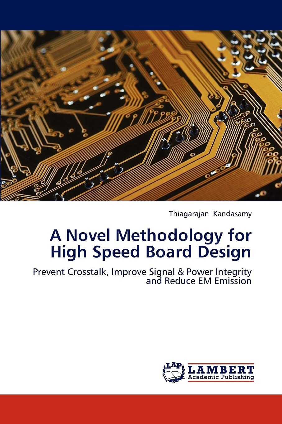
Current highspeed designs demand a board designers extensive knowledge of the issues like transmission line effect, EMI, and crosstalk. Modern PCB design concerned with board material, signal and power stacking, connectors, cables, vias, and trace dimensions. With such designs, the complexity of PCB design increases with the aspects of SI which originate noise and instability. Crosstalk is a major noise that interferes with SI. The noise voltage in the reference or ground of a PCB is often the cause of unwanted radiated emission. Power supply planes attribute to the noise voltage. A Gigabit Ethernet design is developed to analyze various issues on PCB designs like Crosstalk, SI & PI, EMI and Thermal variations. Techniques are investigated to reduce the radiated EM fields, improve power delivery system of the design and eliminate the crosstalk related to routing the high speed signals. SI analysis & thermal analysis help to improve design characteristics. EMI results are within the limits of FCCCLASS B/ VCCICLASS B standards with crosstalk within the limit of 100mV. The design is developed to achieve DFA/DFM/DFT for the manufacturing process of high speed & high dense PCB.
⚠️ WARNING (California Proposition 65):
This product may contain chemicals known to the State of California to cause cancer,
birth defects, or other reproductive harm.
For MAP (Minimum Advertised Price) violations and Intellectual Property (IP) or Trademark concerns, please contact:
support@ergodebooks.com
⚠️ California Proposition 65 Warning: Some products sold on this website may expose you to chemicals known to the State of California to cause cancer, birth defects, or other reproductive harm. For more information, visit www.P65Warnings.ca.gov.